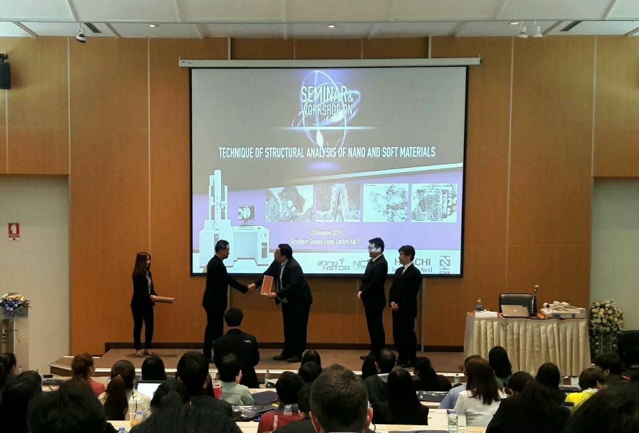
Seminar & Workshop on Technique of Structural Analysis of Nano and Soft Materials.
Last updated: 28 May 2021 | 1953 Views |

In almost all fields of modern science and technology, the demand for high resolution imaging on delicate nanomaterials are becoming ever more challenging. In our upcoming seminar & workshop, we would like to cordially invite you to join us to discover the know-how and techniques to observe and analyze on nano and soft materials, using the new Hitachi HT7800 Low kV Transmission Electron Microscope. Low-kV (20-120 kV) TEM is widely used for observation of light-element specimens, typically in the biomedical field. It has lately attracted in the nanomaterial field as well. Because it has the potential to reduce the knock-on beam damage and enhance contrast.
In case of TEM characterization of composites such as chemically synthesized catalyst, carbon based nanomaterials, oxides and hydroxides, the highest attention should be paid to electron irradiation damage. The selection of an optimal accelerating voltage based on composition is one option to reduce irradiation damage.
In addition, the selected area electron beam diffraction (SAD) technique is one of the preferable techniques in the structural analysis of the Nano composite materials. The example of SAD patterns obtained with a high resolution objective lens and an automatic acquisition function of SAD will be presented. Moreover, we have newly developed a hollow cone dark field TEM image acquisition function to visualize crystal grain distribution of semiconductor materials. Further detail of improved functions for Low-kV TEM equipped with a high resolution objective lens and application results will be presented.

This seminar was sponsored by HITACHI and Coax with NSTIR as the host.
Related content
Powered by
MakeWebEasy.com


