Home > Product > EM/AFM > SEM/TEM/STEM
Electron Microscopes (SEM/TEM/STEM)
A wide array of advanced electron microscopes, including Standard and Variable-Pressure Scanning Electron Microscopes (SEM & VP-SEM), Field-Emission Scanning Electron Microscopes (FE-SEM), Biological and Analytical Transmission Electron Microscopes (TEM), Scanning Transmission Electron Microscopes (STEM), and Tabletop Microscopes

FE-SEM
(Field Emission Scanning Electron Microscopes)
See more details >>
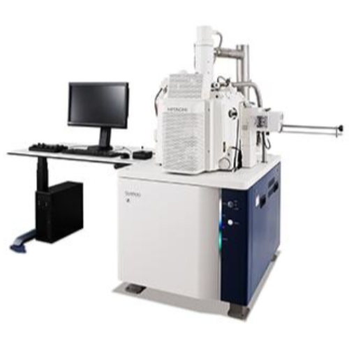
SEM
(Scanning Electron Microscopes)
Conventional SEM employs thermionic electron source (tungsten filament) and can accommodate relatively large sample. Using low vacuum mode, non-conductive sample, outgassing sample, and sample containing a little water or oil can be observed without metal coating. Broad-ranging lineup from compact type to large chamber model is available based on sample size and application.

Tabletop Microscopes

TEM
(Transmission Electron Microscopes)
There are several TEM/STEMs of different accelerating voltages and proper model is used based on the sample composition. 300kV/200kV models with superior resolution and penetrating power are used for inorganic materials such as metals and ceramics while 120kV model with higher contrast is used for polymers and biological tissues. When advanced analytical performances such as nano area analysis and atomic-resolution analysis are required, FE electron source and spherical aberration corrector are powerful options.

Nano-probing System
Nano-probing system is SEM-based probing system optimized for electrical characterization and Electron Beam Absorbed Current (EBAC) analysis of semiconductor devices. High resolution SEM with high-brightness FE electron source enables intuitive operation and precise control of the probes.

AMICS Software (MLA)
AMICS (The Advanced Mineral Identification and Characterization System) is a software package for automated identification and quantification of minerals and synthetic phases. It enables Bruker's QUANTAX EDS on Hitachi SEM to become a fully automated Mineral Liberation Analyzer (MLA).